Scanning electron microscopes (SEMs) are powerful tools for many failure analysis applications because they reveal micro- and nanometer-scale structural details. This feature helps researchers precisely characterize microscopic defects or nanoscale deviations from process specifications, some of which other tools are unable to observe. Using these insights, researchers can identify and recommend quality improvements in the earliest stages of defect formation – and quickly receive results.
Best practices for SEM failure analysis
SEM failure analysis is a diverse area and today’s SEM machines come with a range of easy-to-use and automated solutions to help you receive quick results, without compromising data quality.
High resolution
You can use a SEM to analyze feature sizes from tens of microns to the sub-nanometer scale. This resolution depends on many factors, including the electron source of your SEM. A tungsten SEM, for example, is suitable for analyzing large feature sizes, which are more than one micron in size. This is a sufficient resolution for most characterization tasks. A Field Emission SEM is suited for small feature sizes of the order of one micron or less, going down to the nanometer scale. An in-lens SEM is suitable for analyzing nanomaterials, of the order of 10 nanometers or less.

At Thermo Fisher Scientific, we supply a range of SEMs. Our powerful Verios XHR SEM, is capable of sub-nanometer resolutions from 1 to 30 keV. Our Apreo 2 SEM system provides all-around nanometer or sub-nanometer resolution performance on materials ranging from nanomaterials, powders, catalysts, and nanodevices to bulk magnetic samples. Our Desktop SEMs offer a lower resolution but still, achieve impressive results. Our Phenom Desktop SEM range is capable of resolutions of the order of 15 nm and less, and our Phenom Pharos Desktop SEM can achieve resolutions of up to 2.5 nm.
Comprehensive and speedy information
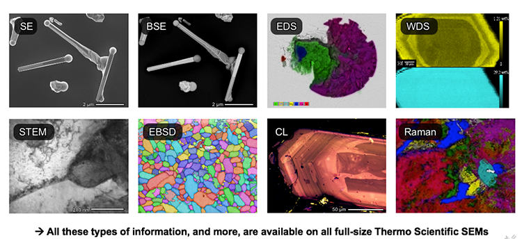
A SEM can provide a wealth of information, compared to optical microscopes, thanks to the versatility of these machines. You can select a range of detectors to meet your requirements and ensure you get all the information you need to complete robust analyses.

A SEM can provide you with data on sample topography, crystallography, impurities, materials contrast, transmission and elemental information.
Elemental information is obtained using Energy Dispersive Spectroscopy (EDS), which gives you quantitative and qualitative information, including the type and concentration of specific elements, while using this technique.
However, when working across multiple measurements, users often have to work across multiple interfaces. This is not only a time-consuming way of work, where you must switch between different interfaces, but it also increases the barriers of entry.
This is where automation and intuitive interfaces can help, completing repetitive tasks and also minimizing your training requirements. Our techniques and tools in this space include:
- Thermo Scientific ChemiSEM Technology is an exclusive live elemental imaging capability. It provides compositional data continuously through one interface. This eliminates several bottlenecks for researchers, compared to conventional EDS, providing ease of use and unparalleled result speed. You can get your elemental information 2-4 times faster using ChemiSEM, compared to conventional technologies.
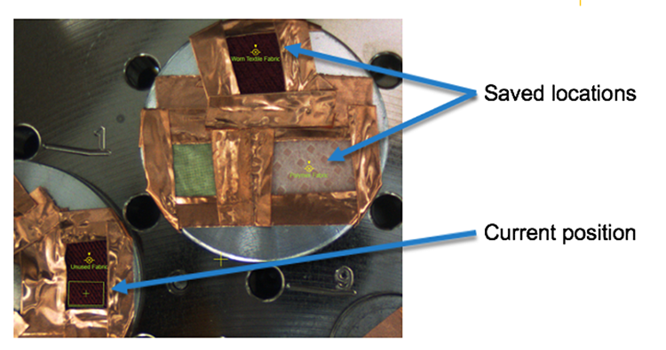
- Using our Nav-cam technology, you can work across multi-sample holders with ease, seamlessly navigating across your samples by marking areas of interest and with a clear indication of your current position.

- Our SmartAlign Technology is a self-aligning optics system, allowing users to guarantee consistency between measurements. This also helps users spend less time on the operation and maintenance of their SEM.
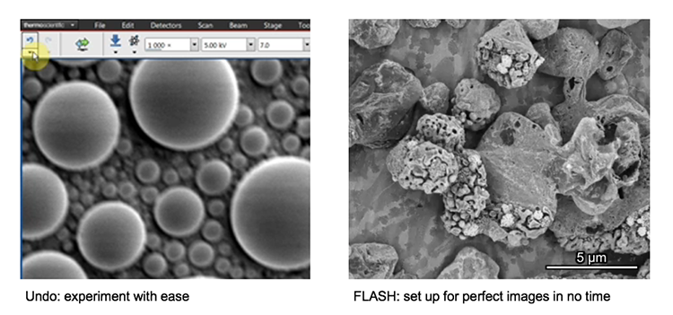
- Using Thermo Scientific FLASH technology, you can automate your image fine-tuning procedures. FLASH Technology can automatically correct the stigmators, lenses centering and the final focus of the image.

Extensive materials tests on difficult samples
SEM failure analysis tests are available across a variety of material types and for a range of materials testing requirements, thanks to the versaility of these machines. You can carry out tests on conducting, insulating, humid and sensitive samples.
Our Environmental SEMs (ESEMs) allow materials to be imaged in their native state. These models are ideally suited for researchers who need to test and analyze samples that are wet, dirty, reactive, outgassing or otherwise not vacuum compatible.
You can also conduct in-situ experiments with an SEM. This is a key capability, where your can conduct direct, real-time observation of microstructural changes to understand the underlying principles of dynamic processes such as recrystallization, grain growth, and phase transformation during heating, cooling, and wetting.
Some quality control examples
The integration of these technologies and tools makes our SEMs easy to operate, ensuring a fast result times regardless of the level of expertise of the end user.
Multi-scale tests
Thanks to the high resolution and multi-scale capabilities of an SEM, researchers can investigate down to the atomic scale and look crystalline formations and grain boundaries, while using EDS to conduct elemental analyses.
For example, battery development is enabled by multi-scale analysis with microCT, SEM and TEM, Raman spectroscopy, XPS, and digital 3D visualization and analysis. This provides the structural and chemical information needed to build better batteries.
Nanoparticles are another key research area and SEM failure analysis application. These materials have fundamentally different properties at the nanoscale than at the macroscale. To study them, S/TEM instrumentation can be combined with energy dispersive X-ray spectroscopy to obtain nanometer, or even sub-nanometer, resolution data.
Particle analysis plays a vital role in nanomaterials research and quality control. The nanometer-scale resolution and superior imaging of electron microscopy can be combined with specialized software for rapid characterization of powders and particles.
Structural analysis
You can identify the root cause of material cracking using an SEM. Cracks generally appear at the micro-scale and along a material’s grain boundaries.
This is a common phenomenon when creating an alloy. When one material is combined with another, granules often appear in the alloy. When the alloy is subjected to stress, cracks can form along the granule boundaries. Eventually, these cracks increase in size until the part fails.
Using SEM failure analysis capabilities, you can view the material’s granules and grain boundaries. This tells you where the cracks are, how they have propagated in the material and provide insights into the root cause of the fault.
This is an important capability within the field of metals research. The effective production of metals requires precise control of inclusions and precipitates. Our automated tools can perform a variety of tasks critical for metal analysis including nanoparticle counting, EDS chemical analysis and TEM sample preparation.
Catalysis research is another key area. Catalysts are critical for a majority of modern industrial processes. Their efficiency depends on the microscopic composition and morphology of the catalytic particles; EM with EDS is ideally suited for studying these properties.
Within polymers research, the material’s microstructure dictates its bulk characteristics and performance. Electron microscopy enables comprehensive microscale analysis of polymer morphology and composition for R&D and quality control applications.
SEM failure analysis – what’s the best option for your lab?
SEMs are powerful and versatile instruments within the world of failure analysis. At Thermo Fisher Scientific, our SEMs have a broad range of features and functionality, from sub-nanometer to microscale resolutions to providing you with the capabilities to extract a wealth of information, all while offering quick results.
Could an SEM optimize your laboratory and boost your failure analysis capabilities? Click here to benchmark your lab’s productivity/versatility to find out more, today.
Electron microscopy services for
the materials science
To ensure optimal system performance, we provide you access to a world-class network of field service experts, technical support, and certified spare parts.
