Semiconductor research and development
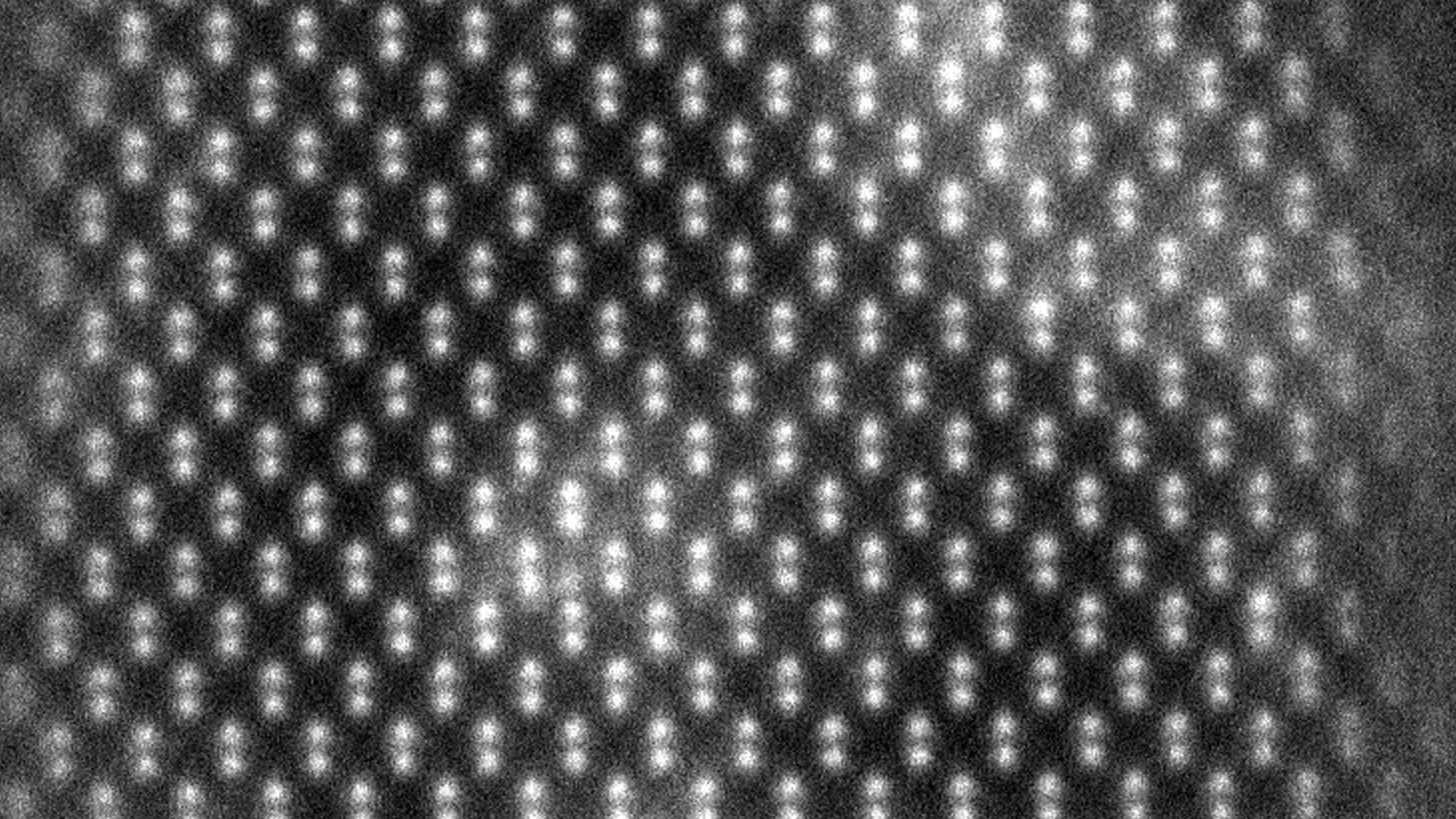
Innovation starts with research and development. Learn more about solutions to help you understand innovative structures and materials at the atomic level.
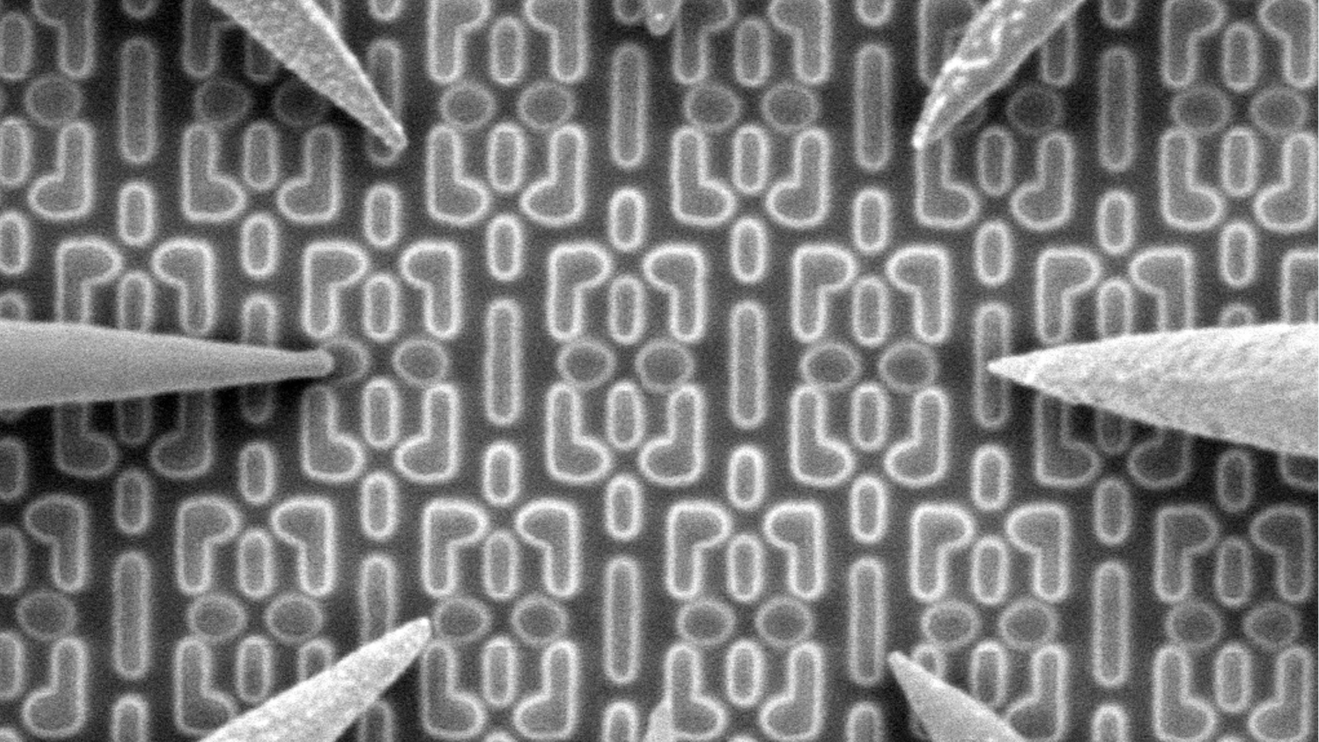
Scanning electron microscopy (SEM) provides high-quality surface and cross-sectional imaging of 3D structures. As semiconductor feature sizes continue to decrease in response to consumer and industry demands, nanoscale metrology becomes an increasingly important contributor to process and device design yield. Accurate and repeatable nanoscale measurements of critical dimensions require high-resolution SEM imaging and extremely accurate magnification calibration.
The ultra-high-resolution automated SEM capabilities offered by Thermo Fisher Scientific, when combined with our industry-leading software solutions, perform imaging and metrology with the automation, precision, and robustness needed to meet the challenges of leading memory and logic customers. Leveraging NIST-traceable calibration standards, mature imaging automation (both cross-sectional and top-down), and next-generation machine-learning-enabled metrology, Thermo Scientific automated SEMs provide cost-effective 3D metrology for direct process and device monitoring, as well as faster time to market.
Thermo Fisher Scientific offers a range of SEM metrology tools for critical dimension analysis, including the Thermo Scientific Verios 5 SEM with Thermo Scientific AutoSEM Software for top-down SEM metrology. Please click through to the appropriate product pages below for more information, or to request a demo.
Innovation starts with research and development. Learn more about solutions to help you understand innovative structures and materials at the atomic level.
Many factors impact yield, performance, and reliability. Learn more about solutions to characterize physical, structural, and chemical properties.
Manufacturing today’s complex semiconductors requires exact process controls. Learn more about advanced metrology and analysis solutions to accelerate yield learnings.
Complex semiconductor device structures result in more places for defects to hide. Learn more about failure analysis solutions to isolate, analyze, and repair defects.
Novel architectures and materials pose new challenges. Learn how to pinpoint faults and characterize materials, structures, and interfaces.
Display technologies are evolving to improve display quality and light conversion efficiency. Learn how metrology, failure analysis, and characterization solutions provide insights.
As semiconductor devices shrink and become more complex, new designs and structures are needed. High-productivity 3D analysis workflows can shorten device development time, maximize yield, and ensure that devices meet the future needs of the industry.
To ensure optimal system performance, we provide you access to a world-class network of field service experts, technical support, and certified spare parts.


