Semiconductor Advanced Packaging
Performance, power efficiency, area, and cost are driving packaging innovations. Learn how workflows provide fast, precise, and accurate time-to-data.
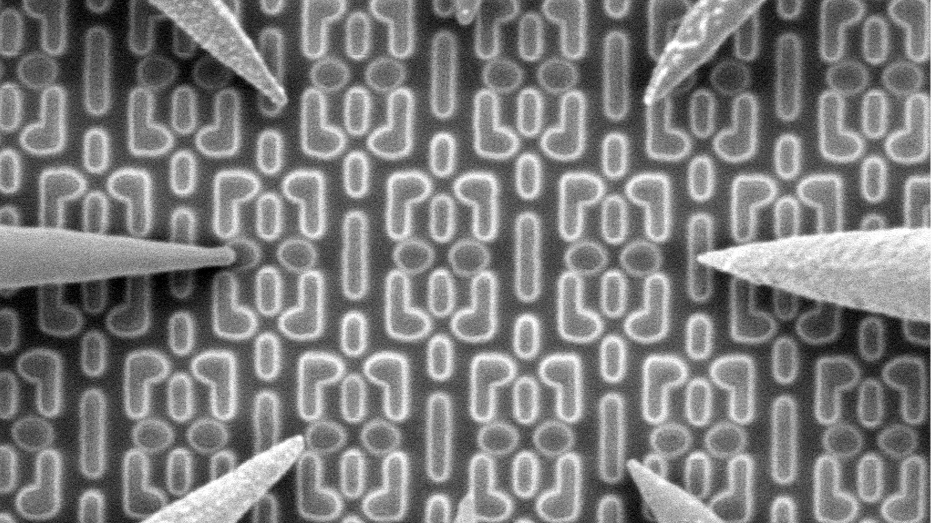
The Thermo Scientific Hyperion II System offers fast, accurate transistor probing for electrical characterization and fault localization in support of semiconductor technology development, yield engineering and device reliability improvement. The unparalleled stability of the Hyperion II System enables nanoprobing down to the 5 nm technology node and beyond.
The Hyperion II System’s SPM technology enables PicoCurrent imaging, which is a technique to rapidly identify shorts, opens, leakage paths and resistive contacts with more than 1,000 times the sensitivity of passive voltage contrast. The scanning capacitance microscopy (SCM) module provides image-based fault localization for silicon on insulator (SOI) wafers, as well as high-resolution dopant profiling.
Capabilities
| Measurement modes The Hyperion II System’s advanced measurement modes include:
|
Probing multiple transistors within the target area to localize a fault can be time-consuming. The Hyperion II System combines PicoCurrent imaging with I-V probing to quickly find potential defects and measure current-voltage curves, without introducing measurement-related shifts.
C-V is used to study oxide layers, interface traps and charge carrier densities. The Hyperion II System offers high-resolution C-V with excellent impedance control, low leakage and very low noise.
Pulsed I-V is used for studying self-heating of SOI and trapped charge in high-k dielectric. The Hyperion II System enables high-speed testing of devices with less than 2 nanosecond rise time.
Integrated PicoCurrent Imaging and Scanning Capacitance Microscopy (SCM) quickly identifies fault candidates for nanoprobing.
Semi-automated step by step guided operation for increased productivity, ease of use and reduced training burden.
Atomic force probes image and probe features, eliminating need for SEM imaging and vacuum system.
Performance, power efficiency, area, and cost are driving packaging innovations. Learn how workflows provide fast, precise, and accurate time-to-data.
Innovation starts with research and development. Learn more about solutions to help you understand innovative structures and materials at the atomic level.
Complex semiconductor device structures result in more places for defects to hide. Learn more about failure analysis solutions to isolate, analyze, and repair defects.
Every electrostatic discharge (ESD) control plan is required to identify devices that are sensitive to ESD. We offer a complete suite of test systems to help with your device qualification requirements.
Novel architectures and materials pose new challenges. Learn how to pinpoint faults and characterize materials, structures, and interfaces.
Many factors impact yield, performance, and reliability. Learn more about solutions to characterize physical, structural, and chemical properties.
Nanoprobing
As device complexity increases, so does the number of places defects have to hide. Nanoprobing provides the precise localization of electrical faults, which is critical for an effective transmission electron microscopy failure analysis workflow.
Nanoprobing
As device complexity increases, so does the number of places defects have to hide. Nanoprobing provides the precise localization of electrical faults, which is critical for an effective transmission electron microscopy failure analysis workflow.
To ensure optimal system performance, we provide you access to a world-class network of field service experts, technical support, and certified spare parts.
